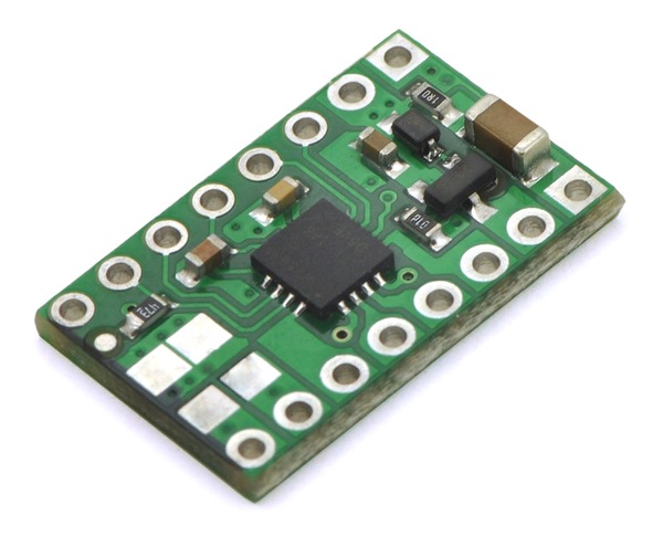
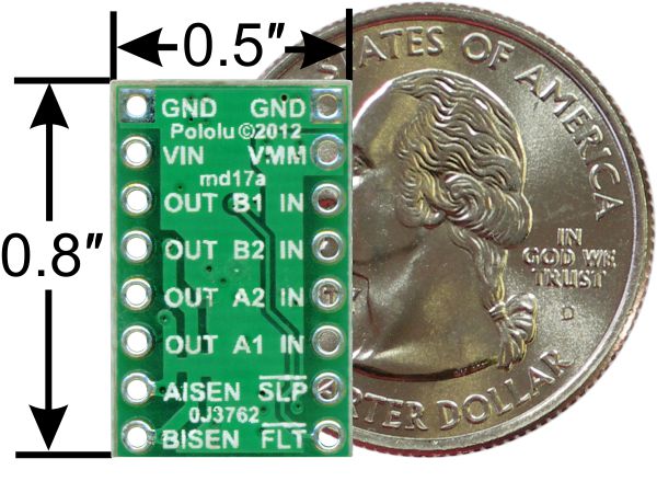
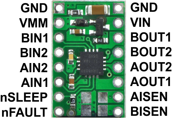
| PIN |
Default State |
Description |
|---|
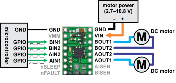
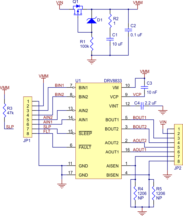
| VIN |
|
2.7–10.8 V motor power supply connection. Operation with VIN below 5 V slightly reduces the maximum current output. |
| VMM |
|
This pin gives access to the motor power supply after the reverse-voltage protection MOSFET (see the board schematic below). It can be used to supply reverse-protected power to other components in the system. It is generally intended as an output, but it can also be used to supply board power. |
| GND |
|
Ground connection points for the motor power supply and control ground reference. The control source and the motor driver must share a common ground. |
| AOUT1 |
|
The motor A half-bridge 1 output. |
| AOUT2 |
|
The motor A half-bridge 2 output. |
| BOUT1 |
|
The motor B half-bridge 1 output. |
| BOUT2 |
|
The motor B half-bridge 2 output. |
| AIN1 |
LOW |
A logic input control for motor channel A. PWM can be applied to this pin. |
| AIN2 |
LOW |
A logic input control for motor channel A. PWM can be applied to this pin. |
| BIN1 |
LOW |
A logic input control for motor channel B. PWM can be applied to this pin. |
| BIN2 |
LOW |
A logic input control for motor channel B. PWM can be applied to this pin. |
| nSLEEP |
HIGH |
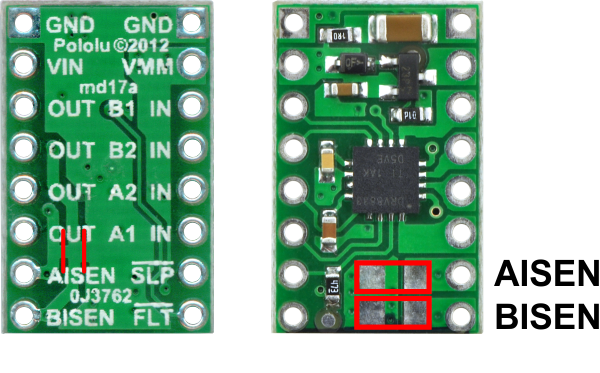
Sleep input: when this pin is driven low, the chip enters a low-power sleep mode. (Labeled SLP on the board silkscreen.) |
| nFAULT |
FLOAT |
Fault output: driven low in the event of an over-current, over-temperature, or under-voltage condition; floating otherwise. (Labeled FLT on the board silkscreen.) |
| AISEN |
|
Current sense pin for motor A. This pin is connected to ground and does not function by default, but current limiting can be enabled by making the modifications described below. |
| BISEN |
|
Current sense pin for motor B. This pin is connected to ground and does not function by default, but current limiting can be enabled by making the modifications described below. |