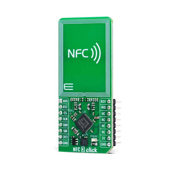
PN5180 NFC 모듈 -13.56Mhz
(NFC 3 CLICK)
개요
- 본 제품은 PN5180 NFC 모듈 -13.56Mhz 입니다.
- PN5180A0HN 칩을 기반으로 디자인된 NFC 모듈로 13.56Mhz에서 동작합니다.
- ISO 14443A/B, ISO 15693, ISO 18092 규격과 호환되며, NFC tag types (type 1, 2, 3, 4A, and 4B)을 읽을 수 있습니다.
특징
-
HOW DOES IT WORK?
NFC 3 Click is based on the PN5180A0HN, a high-performance multiprotocol full NFC frontend from NXP Semiconductors, for contactless communication at 13.56MHz. The PN5180A0HN implements the RF and all the low-level functionality, like an antenna driving and receiver circuitry, to realize an NFC Forum-compliant reader. It utilizes an outstanding modulation and demodulation concept for different contactless communication methods and protocols. The PN5180A0HN is fully compliant with many Reader/Writer standards like ISO 14443A/B up to 848 kBit/s, JIS X 6319-4 comparable with FeliCa scheme, ISO 15693, ISO 18092, and more. Alongside support for reading all NFC tag types (type 1, 2, 3, 4A, and 4B) and high RF output power, this Click board™ is ideally suited for industrial and consumer NFC applications like industrial, eGov readers, payment terminals, and more.
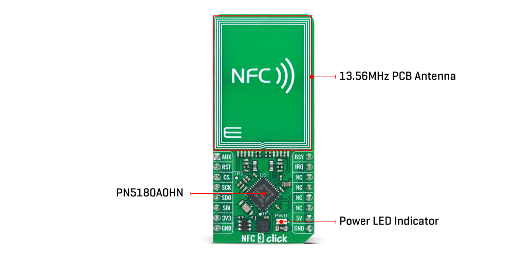
This Click board™ connects to a host MCU with an SPI interface for configuration, NFC data exchange, and high-level NFC protocol implementation. It supports the most common SPI Mode 0 and operates with data rates up to 7 Mbit/s. The PN5180A0HN has two types of integrated memories: RAM and EEPROM. Internal registers of the PN5180A0HN store configuration data, while the RF configuration for dedicated RF protocols is defined by EEPROM data, copied by a command issued from the host MCU. This allows users to achieve maximum RF performance from a given antenna design.
In addition to the SPI interface signals, this board uses several other signals from the mikroBUS™ socket. The reset pin routed on the RST pin of the mikroBUS™ socket provides the general reset ability, while the IRQ pin of the mikroBUS™ socket represents an interrupt request to inform the host controller of various events.
The PN5180A0HN also has the possibility of updating the implemented firmware. In Secure Firmware update mode, the PN5180A0HN requires dedicated physical handling of the SPI interface lines and the BSY line of the mikroBUS™ socket. The BSY signal is used to indicate that the PN5180A0HN is not able to send or receive data over the SPI interface. The secure firmware download mode is entered by setting the AUX pin to a high logic state during the Start-Up sequence of the device. The AUX pin is allowed for any other functionality after Start-Up (as test signals provided by test points on the board); the level of this pin has no impact on the download functionality after Start-Up during standard NFC operation.
This Click board™ can only be operated from a 3.3V logic voltage level. Therefore, the board must perform appropriate logic voltage level conversion before using MCUs with different logic levels. However, the Click board™ comes equipped with a library containing functions and an example code that can be used as a reference for further development.
SPECIFICATIONS
Type RFID/NFC Applications Can be used for industrial and consumer NFC applications like industrial, eGov readers, payment terminals, and more On-board modules PN5180A0HN - multiprotocol NFC frontend from NXP Semiconductors Key Features High performance, full NFC Forum-compliant frontend, contactless communication at 13.56MHz, fully compliant with many Reader/Writer standards, reading of all NFC tag types, SPI interface, high RF power, possibility of updating the implemented firmware, and more Interface SPI Compatibility mikroBUS Click board size L (57.15 x 25.4 mm) Input Voltage 3.3V,5V