3축 가속도 센서 -ADXL367
(ACCEL 22 CLICK)
개요
- 본 제품은 3축 가속도 센서 -ADXL367 입니다.
- ADXL367 칩을 기반으로 디자인된 제품으로 3축에 대해 ±2g, ±4g, ±8g 의 범위의 풀스케일 가속도 측정이 가능합니다.
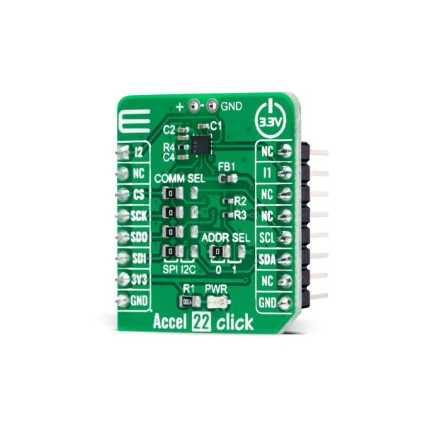
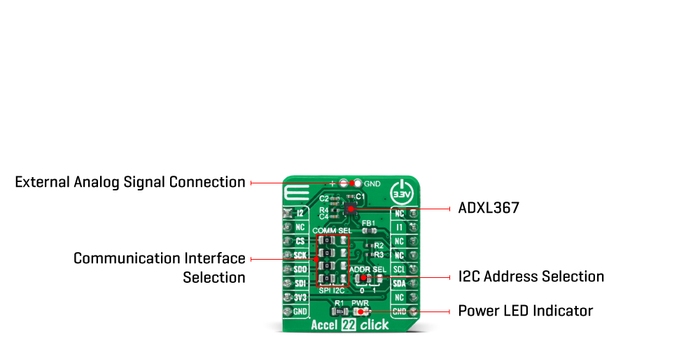
- I2C/SPI 인터페이스를 지원합니다.
- 3.3V 시스템과 사용이 가능합니다.
특징
-
HOW DOES IT WORK?
Accel 22 Click as its foundation uses the ADXL367, a complete 3-axis acceleration measurement system that operates at low power consumption levels, consisting as well of an ADC for synchronous conversion of input from a third sensor and a temperature sensor from Analog Devices. It measures both dynamic accelerations, resulting from motion or shock, and static acceleration, such as tilt, and allows selectable full-scale acceleration measurements in ranges of ±2g, ±4g, and ±8g with a resolution of 0.25mg/LSB on the ±2g range. Acceleration is reported digitally, communicating via either the SPI or the I2C protocol and providing 14-bit output resolution.
The ADXL367 has three operating modes: Measurement mode for continuous wide-bandwidth sensing, Wake-up mode for limited bandwidth activity detection, and Standby mode for power conservation. Measurement mode represents its normal operating mode, and in this mode, acceleration data is read continuously, while the Wake-Up mode is ideal for simple detection of the presence or absence of motion at low power consumption. Wake-up mode helps implement a motion-activated ON/OFF switch, allowing the rest of the system to Power-Down until the activity is detected. In addition, the Standby mode suspends measurement and reduces power consumption.
Accel 22 Click allows using both I2C and SPI interfaces. The selection can be made by positioning SMD jumpers labeled as COMM SEL in an appropriate position. Note that all the jumpers' positions must be on the same side, or the Click board™ may become unresponsive. While the I2C interface is selected, the ADXL367 allows choosing the least significant bit (LSB) of its I2C slave address using the SMD jumper labeled ADDR SEL.
This Click board™ also possesses two register-configurated interrupt pins, I1 and I2, routed to the INT and AN pins on the mikroBUS™, which has a dual function that can trigger interrupts to alert the host of certain status conditions. They can be used as classic interrupt pins to signal MCU that an event has been sensed or can be used, e.g., I1 as an input for external clocking and I2 as input for synchronized sampling. One or both of these alternate functions can be used concurrently; however, if an interrupt pin is used for its alternate function, it cannot simultaneously be used for its primary function, to signal interrupts.
The ADXL367 incorporates a 14-bit analog-to-digital converter (ADC) to digitize the external analog signal, connected to a header at the top of the board, which is unpopulated by default. The ADC converts analog inputs ranging from 10% to 90% of the internally regulated voltage, limiting the external ADC's input range to a maximum of 1V.
This Click board™ can be operated only with a 3.3V logic voltage level. The board must perform appropriate logic voltage level conversion before using MCUs with different logic levels. However, the Click board™ comes equipped with a library containing functions and an example code that can be used, as a reference, for further development.
SPECIFICATIONS
Type Motion Applications Can be used for various applications such as motion-activated functions and user interfaces and many asset monitoring functions in a wide range of industrial applications On-board modules ADXL367 - three-axis MEMS accelerometer from Analog Devices Key Features Low power consumption, high-performance, high resolution, single/double tap detection, adjustable threshold sleep/wake-up modes for motion activation, configurable interrupts, integrated temperature sensor, external analog signal connection, and more Interface I2C,SPI Compatibility mikroBUS Click board size S (28.6 x 25.4 mm) Input Voltage 3.3V