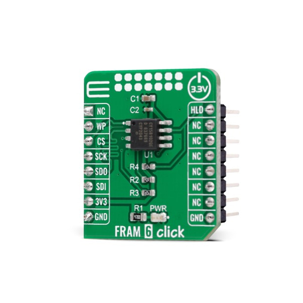
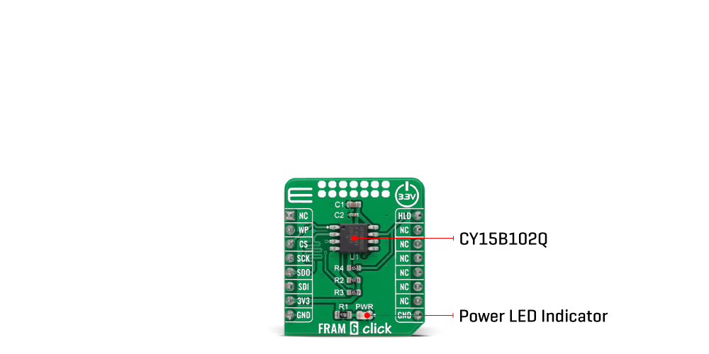
NV FRAM CY15B102Q 모듈 -2Mbit
(FRAM 6 CLICK)
개요
- 본 제품은 NV FRAM CY15B102Q 모듈 -2Mbit 입니다.
- CY15B102Q 칩을 기반으로 디자인된 제품입니다.
- SPI 인터페이스를 통해 읽기/쓰기를 할 수 있습니다.
특징
-
HOW DOES IT WORK?
FRAM 6 Click as its foundation uses the CY15B102Q, a 2Mbit ferroelectric random access memory (F-RAM) logically organized as 262,144×8 bits and accessed using an industry-standard serial peripheral interface from Infineon, now part of Infineon. The functional operation of the F-RAM is similar to serial flash and serial EEPROMs, where the significant difference between the CY15B102Q and a serial flash or EEPROM represents the F-RAM's superior write performance, high endurance, and low power consumption. That's why this Click board™ is ideal for nonvolatile memory applications requiring frequent or rapid writes, where example ranges from data collection to demanding industrial controls where the long write time of serial flash or EEPROM can cause data loss.
The CY15B102Q communicates with MCU through a standard SPI interface that enables very high clock speeds up to 25MHz, supporting the two most common SPI modes, SPI Mode 0 and 3. Unlike serial flash and EEPROM, the CY15B102Q performs write operations at bus speed, where no write delays are incurred. The CY15B102Q supports 10 trillion read/write cycles, or 10 million times more write cycles than EEPROM. Data is written to the memory array immediately after each byte is successfully transferred to the device. The following bus cycle can commence without the need for data polling.
An additional feature of this Click board™ represents the configurable Write Protection function labeled as WP routed on the RST pin of the mikroBUS™ socket. The WP pin protects the entire memory and all registers from write operations and must be set to a high logic state to inhibit all the write operations. All memory and register writes are prohibited when this pin is high and the address counter is not incremented. Besides, the FRAM 6 Click also has an additional HOLD pin, routed to the PWM pin of the mikroBUS™ socket labeled as HLD, to interrupt a serial operation without aborting it.
This Click board™ can be operated only with a 3.3V logic voltage level. The board must perform appropriate logic voltage level conversion before use with MCUs with different logic levels. However, the Click board™ comes equipped with a library containing functions and an example code that can be used, as a reference, for further development.
-
Type FRAM Applications Can be used for nonvolatile memory applications requiring frequent or rapid writes and unlimited endurance On-board modules CY15B102Q - 2Mbit nonvolatile memory employing an advanced ferroelectric process organized as 256K words of 8 bits each from Cypress Semiconductor, now part of Infineon Key Features Low power consumption, high endurance, 121 years data retention, advanced high-reliability ferroelectric process, fast serial interface, sophisticated write protection scheme, and more Interface SPI Compatibility mikroBUS Click board size S (28.6 x 25.4 mm) Input Voltage 3.3V