H-BRIDGE 게이트 드라이버 -MC33883
(H-BRIDGE DRIVER CLICK)
개요
- 본 제품은 H-BRIDGE 게이트 드라이버 -MC33883 입니다.
- MC33883 칩을 탑재하고 있습니다.
- 게이트 드라이버 채널은 독립적으로 4개의 분리된 입력 핀에 의해 제어됩니다.
- 최대 1.0A 피크 전류 펄스까지 소스나 싱크 할 수 있어 large gate-charge MOSFET을 high PWM 주파수로 제어할 수 있게 합니다.
- 3.3V/5V 시스템과 사용이 가능합니다.
특징
-
Type Brushed Applications Can be used for automotive engine applications (electric pumps), energy storage systems (ESS), uninterruptible power supply (UPS), and more. On-board modules MC33883 - H-bridge gate driver (or full-bridge pre-driver) with integrated charge pump and independent high and low-side driver channels from NXP Semiconductors Key Features Full-bridge pre-driver, built-in high side charge pump, UVLO and OVLO features, Sleep mode, PWM up to 100kHz, and more. Interface GPIO Compatibility mikroBUS Click board size L (57.15 x 25.4 mm) Input Voltage 3.3V or 5V,External -
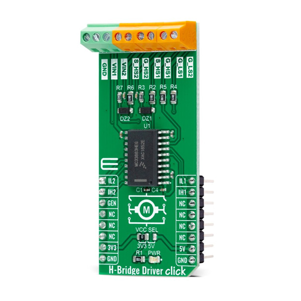
H-Bridge Driver Click as its foundation uses the MC33883, an H-bridge gate driver (or full-bridge pre-driver) with integrated charge pump and independent high and low-side driver channels from NXP Semiconductors. Gate driver outputs can source and sink up to 1.0A peak current pulses, permitting large gate-charge MOSFETs to be driven and/or high pulse-width modulation (PWM) frequencies to be utilized. It also supports a Sleep mode of operation with its low supply current, typical of 10μA.
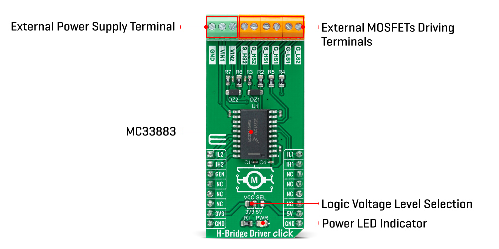
The VIN1 and VIN2 terminals are the power supply inputs to the device. VIN1 is used for the output high-side drivers and the charge pump, while VIN2 is used for the linear regulation. They can be connected together or with different voltage values with VIN1 up to 45V and VIN2 up to 28V. These pins also have undervoltage (UV) and overvoltage (OV) shutdown features. If one of the supply voltage drops below the undervoltage threshold or rises above the overvoltage threshold, the gate outputs are switched low to switch off the external MOSFETs. When the supply returns to a level above the UV threshold or below the OV threshold, the device resumes normal operation according to the established condition of the input pins.
The gate driver channels are independently controlled by four separate pins, routed to the RST, AN, PWM, and INT pins of the mikroBUS™ socket. Those pins allow the device to be optionally configured as two independent high side gate drivers and two independent low side gate drivers. In addition, it also has a pin used to place the device in Sleep mode. When the GEN pin, routed to the CS pin of the mikroBUS™ socket, is in a logic low state, the device is in Sleep mode; otherwise, it is fully operational.
This Click board™ can operate with both 3.3V and 5V logic voltage levels selected via the VCC SEL jumper. This way, it allows both 3.3V and 5V capable MCUs to use the GPIO communication lines properly. However, the Click board™ comes equipped with a library containing easy-to-use functions and an example code that can be used, as a reference, for further development.