NFC RFID 통신 모듈 -PN7150, 13.56Mhz
(NFC 2 CLICK)
개요
- 본 제품은 NFC RFID 통신 모듈 -PN7150 입니다.
- 13.56Mhz NFC 태그와 통신이 가능하며, I2C 인터페이스를 가지고 있습니다.
- PN7150은 ARM Cortex M0 코어를 내장하고 있으며, 다양한 NFC 프로토콜을 지원하는 펌웨어를 탑재하고 있습니다.
- 3.3V/5V 시스템과 사용이 가능합니다.
특징
-
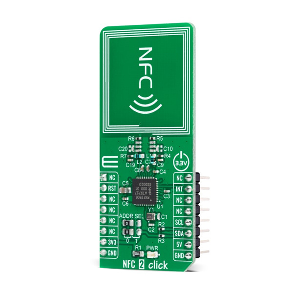
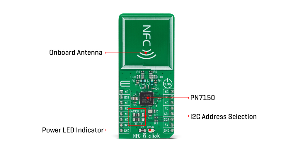
NFC 2 Click is based on the PN7150, high-performance full NFC solution with integrated firmware and I2C interface designed for contactless communication at 13.56 MHz from NXP USA Inc. This board has full compliance with NFC Forum specification that means that you will be able to use the full potential of NFC. It is the ideal solution for rapidly integrating NFC technology in any application, especially those running O/S environments like Linux and Android, reducing size and cost thanks to embedded NFC firmware providing all NFC protocols as a pre-integrated feature and ultra-low power consumption.
The PN7150 embeds a microcontroller core ARM Cortex-M0 loaded with the integrated firmware and provides an easy integration and validation cycle as all the NFC real-time constraints, protocols, and device discovery are being taken care of internally. The host can configure the PN7150 to notify for a card or peer detection and start communicating with them. The core microcontroller chip of the PN7150 can run without any external clock (based on an internal oscillator). However, the 13.56MHz RF field carrier accuracy requirements are not compatible with the use of an internal oscillator. That’s why the PN7150 has an external crystal oscillator connected to its XTAL pins.
It also has four power states: Monitor, Hard Power Down (HPD), Standby, and Active. At the application level, the PN7150 will continuously switch between different power states to optimize the current consumption. The PN7150 is designed to allow the host controller to have full control over its operation, thus of the power consumption of the PN7150 based NFC solution and the possibility to restrict parts of the PN7150 functionality. More information about these modes user can find in the attached datasheet.
NFC 2 Click communicates with MCU using the standard I2C 2-Wire interface with a clock frequency up to 100kHz in the Standard, up to 400kHz in the Fast, and up to 3.4MHz in the High-Speed Mode. The PN7150 also allows the choice of the least significant bit (LSB) of its I2C slave address by positioning SMD jumpers labeled as ADDR SEL to an appropriate position marked as 0 and 1. To enable and ensure data flow control between PN7150 and host controller, additionally, a dedicated interrupt line labeled as INT is provided that Active state is programmable. It also contains Reset function, and the RF antenna which is used to communicate over RF with a Tag (Card) and a Reader/Writer or a Peer device.
This Click board™ is designed to be operated only with a 3.3V logic voltage level, while 5V is used as transmitter input supply voltage of PN7150. A proper logic voltage level conversion should be performed before the Click board™ is used with MCUs with different logic levels. However, the Click board™ comes equipped with a library that contains easy to use functions and an example code which can be used, as a reference, for further development.
-
Type RFID/NFC Applications Can be used for rapidly integrating NFC technology in any application. On-board modules NFC 2 Click is based on the PN7150, high-performance full NFC solution with integrated firmware and I2C interface designed for contactless communication at 13.56 MHz from NXP USA Inc. Key Features Ultralow power consumption, automatic wake-up via RF field, integrated non-volatile memory to store data and executable code for customization, various RF protocols supported, includes ARM Cortex-M0 microcontroller core, and more. Interface I2C Compatibility mikroBUS Click board size L (57.15 x 25.4 mm) Input Voltage 3.3V or 5V