벅 컨버터 -LT3976 스텝다운 모듈
(BUCK click)
개요
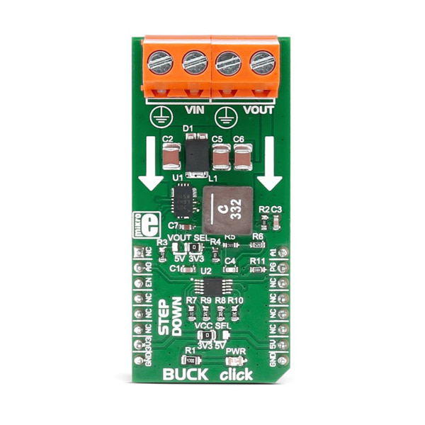
- 본 제품은 LT3976 40V, 5A, 2MHz step-down switching regulator 를 탑재한 DC-DC 스텝 다운 모듈입니다.
- 40V까지의 입력을 3.3V나 5V로 다운 시켜 줍니다.
- 적절하게 열을 식혀주고 최적으로 셋팅한다면 최대 5A까지의 전류를 처리할 수 있습니다.
특징
-
LT3976 regulator features
The LT3976 is an adjustable frequency monolithic buck switching regulator that accepts a wide input voltage range up to 40V. Low quiescent current design consumes only 3.3µA of supply current while regulating with no load. Low ripple Burst Mode operation maintains high efficiency at low output currents while keeping the output ripple below 15mV in a typical application.
The LT3976 can supply up to 5A of load current and has current limit foldback to limit power dissipation during short-circuit. A low dropout voltage of 500mV is maintained when the input voltage drops below the programmed output voltage, such as during automotive cold crank.
How the click works
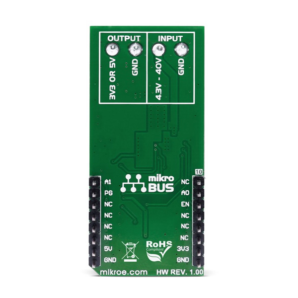
There are two onboard screw terminals, one for connecting the external input supply, and the other for the output. There is also a multiplexer which chooses the resistor used for setting the switching frequency.
.jpg)
The multiplexer is used for selecting one of the four different resistors. Each of these resistors, if selected, sets different switching frequency:
A0 A1 Selects resistor Switching frequency [MHz] 0 0 R7 = 130k 0.4 0 1 R8 = 32.4k 1.2 1 0 R9 = 54.9k 0.8 1 1 R10 = 21.5k 1.6 Specifications
Type Buck Applications Automotive battery regulation, portable devices, industrial supplies, etc. On-board modules LT3976 step-down switching regulator, MAX4634 4-channel CMOS analog multiplexer Key Features Thermal shutdown protection, output voltage can be set to 3.3V or 5V, 4 possible switching frequencies Interface GPIO Input Voltage 3.3V or 5V Click board size L (57.15 x 25.4 mm) Pinout diagram
This table shows how the pinout on BUCK click corresponds to the pinout on the mikroBUS™ socket (the latter shown in the two middle columns).
Notes Pin 
Pin Notes NC 1 AN PWM 16 A1 Multiplexer A1 pin Multiplexer A0 pin A0 2 RST INT 15 PG Open drain output of an internal comparator Enable IC EN 3 CS TX 14 NC NC 4 SCK RX 13 NC NC 5 MISO SCL 12 NC NC 6 MOSI SDA 11 NC Power supply +3.3V 7 3.3V 5V 10 +5V Power supply Ground GND 8 GND GND 9 GND Ground Jumpers and settings
Designator Name Default Position Default Option Description JP1 VOUT SEL Right 3V3 Output Voltage Selection 3V3/5V, left position 5V, right position 3V3. JP2 VCC SEL Left 3V3 Power Supply Voltage Selection toward host MCU 3V3/5V; left position 3V3, right position 5V
문서
연관제품
- 연관제품 1