설정가능 8채널 12비트 ADC, DAC, GPIO 모듈 -AD5593R
(ADAC click)
개요
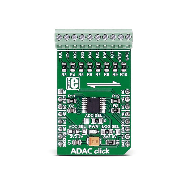
- 본 제품은 8개의 채널을 가진 12비트 ADC, DAC, GPIO 모듈입니다.
- ADC/DAC를 설정가능한 AD5593R 를 탑재하고 있으며, 3.3V, 5V와 사용이 가능합니다.
- MCU와는 I2C 인터페이스를 이용하여 통신합니다.
- 각각의 채널은 개별적으로 ADC, DAC, GPIO로 설정이 가능하며, 12비트로 변환된 값은 I2C를 통해 읽을 수 있습니다.
특징
-
AD5593R IC features
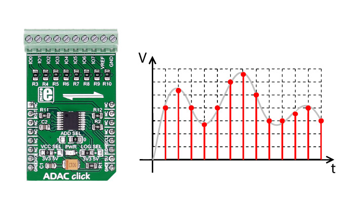
The AD5593R has eight input/output (I/O) pins, which can be independently configured as digital-to-analog converter (DAC) outputs, analog-to-digital converter (ADC) inputs, digital outputs, or digital inputs. When an I/O pin is configured as an analog output, it is driven by a 12-bit DAC. The output range of the DAC is 0 V to VREF or 0 V to 2×V REF.
When an I/O pin is configured as an analog input, it is connected to a 12-bit ADC via an analog multiplexer. The input range of the ADC is 0 V to VREF or 0 V to 2 × VREF. The I/O pins can also be configured to be general-purpose, digital input or output (GPIO) pins.
Specifications
Type ADC Applications control and monitoring, measurement, etc. On-board modules AD5593R 8-Channel, 12-Bit, Configurable ADC/DAC Key Features 8 12-bit DAC channels, 8 12-bit ADC channels Interface GPIO,I2C Peripherals include Screw terminals Input Voltage 3.3V or 5V Compatibility mikroBUS Click board size M (42.9 x 25.4 mm) Key features
- AD5593R configurable ADC/DAC
- 8 12-bit DAC channels
- 8 12-bit ADC channels
- 8 general-purpose I/O pins
- I2C interface
- 3.3V or 5V power supply
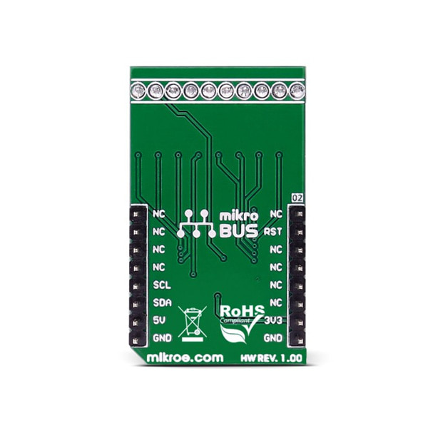
Pinout diagram
This table shows how the pinout on ADAC click corresponds to the pinout on the mikroBUS™ socket (the latter shown in the two middle columns).
Notes Pin 
Pin Notes NC 1 AN PWM 16 NC Active low IC reset RST 2 RST INT 15 NC NC 3 CS TX 14 NC NC 4 SCK RX 13 NC NC 5 MISO SCL 12 SCL I2C serial clock NC 6 MOSI SDA 11 SDA I2C serial data Power supply +3.3V 7 3.3V 5V 10 +5V Power supply Ground GND 8 GND GND 9 GND Ground Additional pins
Name I/O Description IO0 Multipurpouse IO pin(ADC,DAC,GPIO)channel0 IO1 Multipurpouse IO pin(ADC,DAC,GPIO)channel1 IO2 Multipurpouse IO pin(ADC,DAC,GPIO)channel2 IO3 Multipurpouse IO pin(ADC,DAC,GPIO)channel3 IO4 Multipurpouse IO pin(ADC,DAC,GPIO)channel4 IO5 Multipurpouse IO pin(ADC,DAC,GPIO)channel5 IO6 Multipurpouse IO pin(ADC,DAC,GPIO)channel6 IO7 Multipurpouse IO pin(ADC,DAC,GPIO)channel7 VREF OPTIONAL Used as input for connecting external VREF or output 2.5V from internal GND OPTIONAL Used for external connection to GND if VREF input is used Jumpers and settings
Designator Name Default Position Default Option Description ADD SEL Address bit 0 3V3 I2C slave address selection, set LSB of slave address 0010001x left pos, 0010000x right pos, (x=R/W) VCC SEL Power supply 3V3 Supply Voltage Selection 3V3/5V, left position 3v3, right position 5v LOG SEL Interface power supply 3V3 Logic Level Voltage Selection 3V3/5V, left position 3v3, right position 5v - AD5593R configurable ADC/DAC
문서
연관제품
- 연관제품 1