블루투스 4.2 듀얼 BT/BLE 모듈 -RN4678
(RN4678 click)
개요
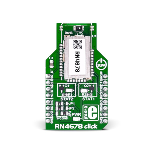
- 본 제품은 Microchip사의 RN4678 블루투스 4.2 듀얼 모드(BT/BLE) 모듈을 탑재한 제품입니다.
- 3.3V에서 동작할 수 있게 디자인되었으며, 마이크로컨트롤러와 I2C, UART 인터페이스로 통신합니다.
특징
-
RN4678 module features
The RN4678 from Microchip is a fully certified, Bluetooth version 4.2 module. Use it to add Bluetooth wireless capability to your project.
The module includes an on-board Bluetooth stack, power management subsystem, 2.4 GHz transceiver, and RF power amplifier.
Data transfer is achieved through the Bluetooth link by sending or receiving data through SPP in Bluetooth (BT) Classic mode and through Transparent UART in the BLE mode.
The RN4678 contains an integral ceramic chip antenna.Strong encryption
The RN4678 module has strong AES128 Encryption. A 128-bit encryption is one of the most powerfull encryption algorithms. AES stands for Advanced Encryption Standard and it is a symmetric encryption algorithm.
Specifications
Type Bluetooth,BLE Applications Internet of Things (IoT), secure payment, home and security, health and fitness, industrial and data logger, LED lighting, etc. On-board modules RN4678 module from Microchip Key Features Frequency: 2.402 GHz to 2.480 GHz, RX Sensitivity: -90 dBm (BR/EDR), -92 dBm (LE), Bluetooth SIG 4.2 Qualified Interface UART,GPIO,I2C Input Voltage 3.3V Compatibility mikroBUS Click board size M (42.9 x 25.4 mm) Pinout diagram
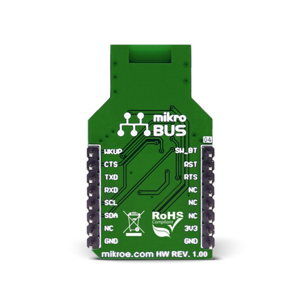
This table shows how the pinout on RN4678 click corresponds to the pinout on the mikroBUS™ socket (the latter shown in the two middle columns).
Notes Pin 
Pin Notes Software Button SW_BTN 1 AN PWM 16 WKUP Wake-up from Sleep mode Module Reset (internal pull-up). Apply a pulse of at least 63 ns. RST_N 2 RST INT 15 CTS Clear To Send Configurable Control or Indication pin or UART RTS (output) RTS 3 CS TX 14 TXD UART data output NC 4 SCK RX 13 RXD UART data input NC 5 MISO SCL 12 SCL I2C Clock NC 6 MOSI SDA 11 SDA I2C Data Power supply +3.3V 7 3.3V 5V 10 NC Ground GND 8 GND GND 9 GND Ground Jumpers and Settings
Designator Name Default Position Default Option Description JP1 P2_0 Left Low System configuration pin - Along with P2_4 and EAN pins, used to set the module in any of the following three modes: Application mode (for normal operation), Test mode (to change EEPROM values), and Write Flash mode (to enter the new firmware into the module); JP2 P2_4 Left Low System configuration pin - Along with P2_0 and EAN pins, used to set the module in any of the following three modes: Application mode (for normal operation), Test mode (to change EEPROM values), and Write Flash mode (to enter new firmware into the module); JP3 EAN Right High External address-bus negative pin. System configuration pin along with P2_0 and P2_4 pins, used to set the module in any of the following three modes: Application mode (for normal operation), Test mode (to change EEPROM values), and Write Flash mode (to enter new firmware into the module);
문서
연관제품
- 연관제품 1