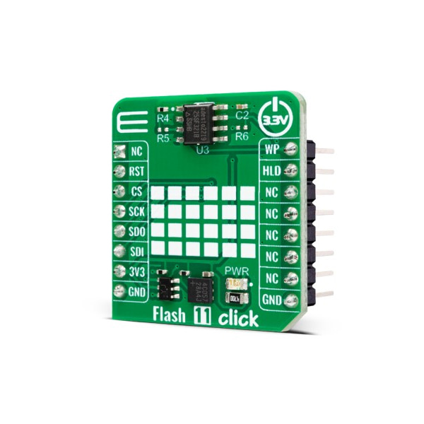
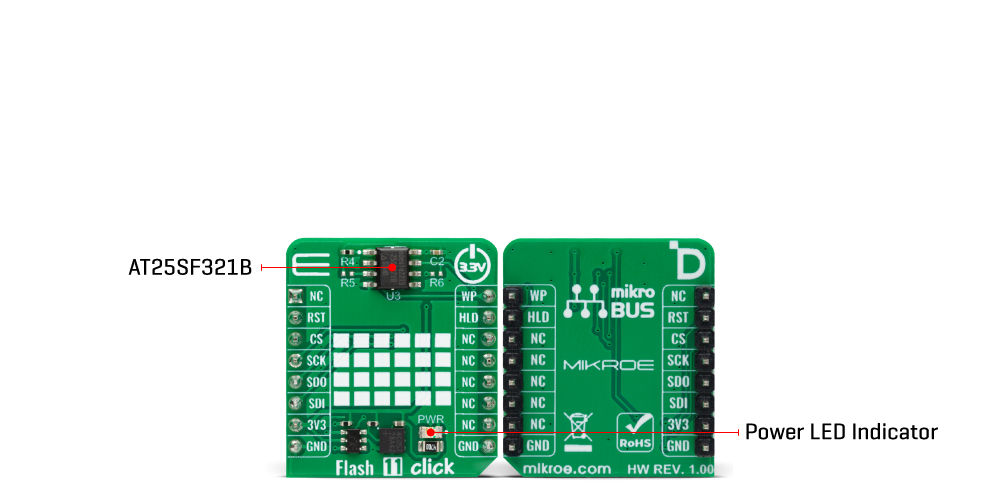
32Mbit SPI 시리얼 플래쉬 메모리 -AT25SF321B
(FLASH 11 CLICK)

개요
- 본 제품은 32Mbit SPI 시리얼 플래쉬 메모리 -AT25SF321B입니다.
- AT25SF321B SPI 플래쉬를 탑재하고 있습니다.
- 3개의 OTP 보안 레지스터를 가지고 있습니다.
특징
-
HOW DOES IT WORK?
Flash 11 Click is based on the AT25SF321B, a 32-Mbit SPI serial Flash memory with Dual I/O and Quad I/O support from Dialog Semiconductor. The AT25SF321A is organized as a 32Mbit (4Mx8 physical block) Flash memory where the memory array can be erased in four levels of granularity, including a full-chip erase, which depending on the blocks, can be done typically in 10 seconds. In addition, the optimized erase architecture allows erasing data in 4kB, 32kB, and 64kB block erase operations. Optimizing the erase blocks' size can be the most efficient use of memory space. The AT25SF321B specifies a minimum of 100.000 endurance cycles with data retention of a minimum of 20 years, allowing it to handle (almost) unlimited reads/writes to the memory.

Flash 11 Click communicates with MCU through a standard SPI interface supporting the two most common SPI modes, SPI Mode 0 and 3, and a maximum clock frequency of up to 108MHz. Furthermore, this Click board™ provides additional hardware-controlled functions. The configurable Write Protection, marked as WP and routed on the default position of the PWM pin of the mikroBUS™ socket, protects all registers (including status and configuration) from write operations and must be held low to inhibit all the write operations to registers. When this pin is in a low logic state, all memory and register write are prohibited, and the address count is not incremented. In addition, there is software write protection too.
Also, it is possible to use the Reset or Hold function through the RST pin of the mikroBUS™ socket, depending on the state of the HOLD/RESET bit 7 in Status Register 3. In the case of the Hold function, this pin temporarily pauses serial communication without deselecting or resetting the device, while in the case of the Reset feature, a low logic level on the RST pin puts the AT25SF321B into a Reset state. This is a part of the Program and Erase, Suspend, and Resume features of the Flash 11 Click.
This Click board™ can be operated only with a 3.3V logic voltage level. The board must perform appropriate logic voltage level conversion before using MCUs with different logic levels. However, the Click board™ comes equipped with a library containing functions and an example code that can be used, as a reference, for further development.
SPECIFICATIONS
Type FLASH Applications Can be used for storage and data transfer in consumer devices, and industrial applications On-board modules AT25SF321B - a 32-Mbit SPI serial Flash memory with Dual I/O and Quad I/O support from Dialog Semiconductor Key Features 32Mbit (4Mx8 memory organization) flash memory, optimized erase architecture for code and data storage applications, flexible non-volatile block protection, high protection, write protection (both hardware and software), data endurance and retention, low power consumption, and more Interface QSPI,SPI Compatibility mikroBUS Click board size S (28.6 x 25.4 mm) Input Voltage 3.3V