16비트 DAC 모듈 -AD3541R
(DAC 13 CLICK)
개요
- 본 제품은 16비트 DAC 모듈 -AD3541R입니다.
- 고정 2.5V 리퍼런스와 동작하는 AD3541R 칩을 기반으로 디자인된 제품입니다.
- SPI 인터페이스를 가지고 있습니다.
- 솔더 점퍼를 설정하여 3.3V/5V 시스템과 사용이 가능합니다.
특징
-
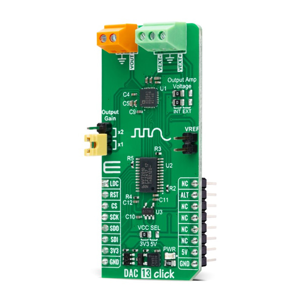
DAC 13 Click is based on the AD3541R, a single channel, 16-bit, 16-MUPS voltage output DAC from Analog Devices, with programmable output ranges. It uses a current-steering DAC architecture with a reference voltage of 2.5V (internal but also with the possibility of an external reference voltage supplied on the VREF header), where DAC current is converted to a voltage through an internal transimpedance amplifier (TIA). The AD3541R also features multiple error-checkers in analog and digital domains to guarantee safe operation in various applications such as data acquisition systems, process control equipment, and many more.
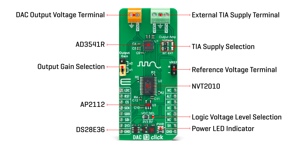
The AD3541R has five pre-configured output voltage ranges: 0V to 2.5V; 0V to 5V; 0V to 10V; −5V to +5V; and −2.5V to +7.5V. The selection of the output range requires a combination of register configurations and a given transimpedance gain (x1 or x2 Output Gain jumper position). These drift-compensating feedback resistors, or transimpedance gain, for the internal TIA, scale the output voltage. The supply for the TIA, integrated into AD3542R, must be adjusted depending on the selected output span. In addition to the internal TIA supply, the user is provided with the possibility of an external trans-impedance amplifier supply on the connector marked with VEXT. Selection can be performed by an onboard SMD jumper labeled as Output Amp Voltage, by placing it to an appropriate position marked as INT or EXT.
This Click board™ communicates with MCU through a versatile SPI interface capable of operating in classic and dual SPI modes with a single or double data rate. The AD3541R has two update modes offering maximum speed and maximum accuracy, synchronously or asynchronously. A synchronous update occurs when the change of the DAC output is triggered by an external LDC signal routed to the AN pin of the mikroBUS™ socket, which with its low state, causes the DAC register to update if the input register has new data, Otherwise, the DAC automatically updates when new data is written to the input register (LDC high). An asynchronous update occurs when the change of the DAC output follows an operation on the register set.
The AD3541R also possesses an additional interrupt alert signal, routed on the INT pin of the mikroBUS™ socket labeled as ALT, indicating abnormal conditions both in the analog and digital domains, and general reset function routed on the RST pin of the mikroBUS™ socket. The ALT pin is also asserted (asserted is incorrect, but I do not know what is meant by this) after reset and in case of initialization failure.
This Click board™ can operate with both 3.3V and 5V logic voltage levels selected via the VCC SEL jumper. A logic voltage level conversion is performed by an appropriate voltage level translator, while an onboard LDO, the AP2112, ensures recommended supply voltage level to power the AD3541R. However, the Click board™ comes equipped with a library containing easy-to-use functions and an example code that can be used, as a reference, for further development.
SPECIFICATIONS
Type DAC Applications Can be used for DAC applications in data acquisition systems, process control equipment, programmable voltage sources, and more On-board modules AD3541R - single channel voltage output digital-to-analog converter (DAC) from Analog Devices Key Features Multiple voltage span ranges, 16-bit resolution, internal or external voltage reference, selectable TIA gain, external or internal TIA supply, precision and accuracy, SPI interface, multiple error detectors, and more Interface SPI Compatibility mikroBUS Click board size L (57.15 x 25.4 mm) Input Voltage 3.3V or 5V
문서
연관제품
- 연관제품 1