32비트 ADC 모듈 -ADS1262
(ADC 13 CLICK)
개요
- 본 제품은 32비트 ADC 모듈 -ADS1262입니다.
- ADS1262 칩을 탑재하고 있습니다.
- SPI 인터페이스를 가지고 있으며, 3.3V 시스템에서 사용이 가능합니다.
특징
-
Type ADC Applications Can be used for the most demanding sensor applications, including weighing scales, strain-gauge sensors, thermocouples, and resistance temperature devices (RTD) On-board modules ADS1262 - low noise, low-drift, 38.4kSPS, delta-sigma (ΔΣ) ADC with an integrated PGA, reference, and internal fault monitors from Texas Instruments Key Features Low power consumption, low noise and drift, integrated PGA, internal fault monitors, 11 multifunction analog inputs, high accuracy, and more Interface SPI Compatibility mikroBUS Click board size M (42.9 x 25.4 mm) Input Voltage 3.3V or 5V -
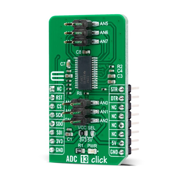
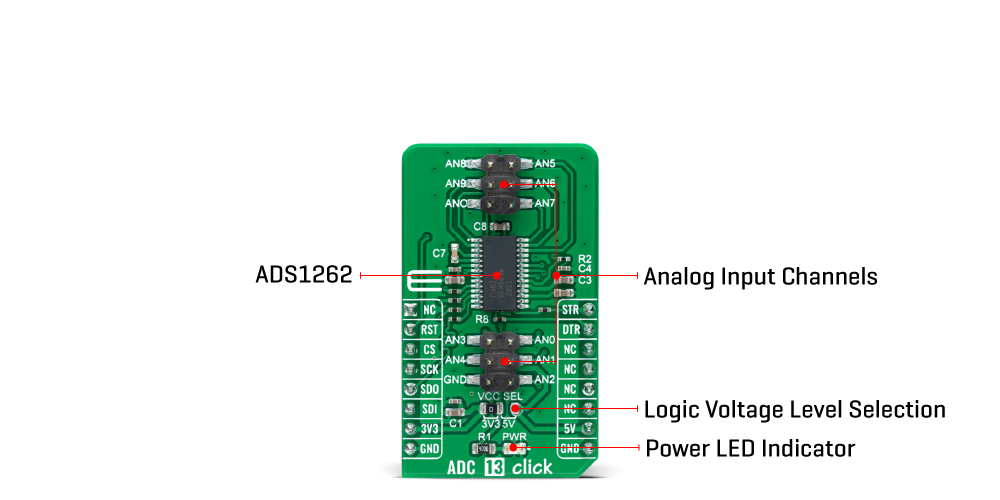
ADC 13 Click as its foundation uses the ADS1262, a low noise, low-drift, 38.4kSPS, delta-sigma (ΔΣ) ADC with an integrated PGA, reference, and internal fault monitors from Texas Instruments. This 32-bit ADC provides output data rates from 2.5 to 38400SPS for flexibility in resolution and data rates over various applications. The ADC's low noise and low drift architecture make these devices suitable for the precise digitization of low-level transducers, such as load cell bridges and temperature sensors.
Following the input multiplexer, ADS1262 features a high-impedance CMOS, a programmable gain amplifier, which provides a low voltage and current noise, enabling direct connection to low-level transducers. The PGA gain is programmable from 1 to 32V/V in binary steps, can be bypassed to allow the input range to extend below ground, and has voltage overrange monitors to improve the integrity of the conversion result.
The ADS1262 communicates with MCU using the standard SPI serial interface with a maximum frequency of 8MHz to read the conversion data, configure and control the ADC. ADC conversions, which can be programmed to a free-run mode or perform one-shot conversions, are started by a control STR pin, routed to the PWM pin of the mikroBUS™ socket, or by commands. An additional ready signal, routed on the INT pin of the mikroBUS™ socket labeled as DTR, is added, indicating that new data is ready for the host. Alongside this pin, this Click board™ has a Reset feature routed to the RST pin on the mikroBUS™ socket, which with a low logic level puts the module into a Reset state, and with a high level operates module normally.
In addition to the ADS1262 present on the ADC 13, this Click board™ also has two 2x3 male headers. Eleven analog inputs located on these headers are configurable as either ten single-ended inputs, five differential inputs, or any combination. Many of the analog inputs are multifunction as programmed by the user.
This Click board™ can operate with both 3.3V and 5V logic voltage levels selected via the VCC SEL jumper. This way, it is allowed for both 3.3V and 5V capable MCUs to use the SPI communication lines properly. However, the Click board™ comes equipped with a library containing easy-to-use functions and an example code that can be used, as a reference, for further development