16Mbit SPI NOR 플래쉬 메모리 -GD25LQ16C
(FLASH 7 CLICK)
개요
특징
-
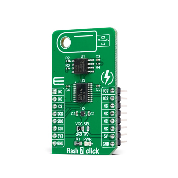
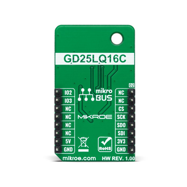
Flash 7 Click is based on the GD25LQ16C, a high-performance 16Mbit SPI NOR Flash Memory solution with advanced security features from GigaDevice Semiconductor. Requiring only 6 signals to communicate between the MCU and the memory thus reduces the design complexity and offers a reduction in board space and total system cost. It is specifically designed to meet the different needs in various electronic applications in terms of density, performance, reliability, and security while providing low power consumption.
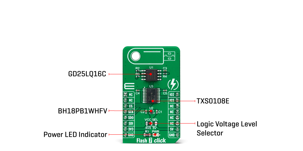
This Click board™ includes an LDO regulator BH18PB1WHFV from Rohm Semiconductor to provide the 1.8 V supply voltage. The LDO cut power consumption by lowering its current consumption to approximately 2 μA when the application is operating in the standby state. The output from the LDO regulator is providing a needed reference voltage for one side of the TXS0108E, an 8-bit bidirectional level shifting and voltage translator for open-drain and push-pull applications from Texas Instruments. The reference voltage for the other side of the level shifter is taken from the 3.3V pin from the mikroBUS™.
Flash 7 Click communicates with MCU using the SPI serial interface that supports the Dual/Quad SPI and the two most common modes, SPI Mode 0 and 3, with a maximum SPI frequency of 104 MHz. The Dual I/O data is transferred with a speed of 208 Mbits/s, and the Quad I/O data with a speed of 416 Mbits/s. In addition to the SPI communication, the Flash 7 Click also has two additional pins used for Write Protection and HOLD function routed to the PWM and INT pins of the mikroBUS™ socket.
The HOLD pin, labeled as IO3, can be used to pause the serial communication with the device without having to stop the operation of write status register, programming, or erasing in progress. On the other side, the configurable Write Protection function labeled as IO2 serves to protect the memory array contents via the Software Protection Mode.
This Click board™ is designed to operate with both 3.3V and 5V logic voltage levels selected via the VCC SEL jumper. It allows for both 3.3V and 5V capable MCUs to use the SPI communication lines properly. However, the Click board™ comes equipped with a library that contains easy to use functions and an example code which can be used, as a reference, for further development.
-
Type FLASH Applications Can be used to provides a storage solution for systems with limited space in various embedded applications. On-board modules Flash 7 Click is based on the GD25LQ16C, a high-performance SPI NOR Flash Memory solution with advanced security features from GigaDevice Semiconductor. Key Features Low power consumption, high performance, reliability, advanced security features, data retention, and more. Interface QUAD ,SPI Compatibility mikroBUS Click board size M (42.9 x 25.4 mm) Input Voltage 3.3V or 5V