DRV8833 Dual Motor Driver Carrier
(DRV8833 듀얼 모터 드라이버)
개요
- 본 보드는 TI사의 DRV8833 듀얼 모터 드라이버를 장착한 보드로 두개의 DC모터에 채널당 1.2A 연속전류(피크시 2A)를 보낼 수 있습니다.
- DRV8833칩은 dual H-bridge motor driver IC로 두개의 브러쉬 DC모터에 대해 양방향 제어를 할 수 있습니다.
- 동작전압은 2.7V~10.8V이며 역전압, 저전압, 과전류, 과열에 대한 자체 보호 기능이 있습니다.
- 본 제품은 작고 저전압 모터를 제어하는데 훌륭한 솔루션입니다.
기능
- Dual H-bridge 모터 드라이버: 두개의 DC모터 혹은 한개의 스텝퍼 모터 동작가능
- 동작 전압: 2.7–10.8 V
- 출력 전류: 모터당 연속 전류 1.2 A (2 A peak)
- 모터 출력은 한개의 모터에 2.4A의 연속 전류 출력이 가능(피크시 4A)
- 입력은 3V, 5V 호환
- 저전압, 과전류, 과열 보호 기능
- 역전압 보호 회로
- sense resistor 추가하여 전류 제한 가능
모터 드라이버 사용하기
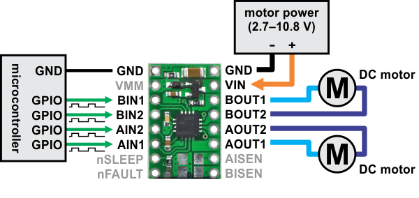
- 일반적인 어플리케이션에서 파워 연결은 보드의 한쪽에, 다른 한쪽에는 제어 연결이 이루어 집니다.
- nSLEEP 핀은 보드상에서 pull high된 상태이며, DRV8833의 저전력 슬립모드를 사용하지 않는다면 연결하지 않아도 됩니다.
- 각각의 모터 채널은 각각 xIN1, xIN2 제어 입력을 가지고 있고, 입력은 대응하는 xOUT1, xOUT2을 설정하게 됩니다.
- PWM신호는 이 입력신호에 적용됩니다.
- 내부적으로 제어 입력은 pull low된 상태로 모터 드라이버 출력을 디폴트로 비활성화 합니다.
- 입력이 어떻게 드라이버 출력에 영향을 미치는지 확인하려면 DRV8833의 데이터쉬트를 참고하십시오.
- nFAULT 핀은 opne-drain 출력으로 과전류, 과열, 저전압 상황이 발행하면 칩에 의해 low로 변경됩니다. 그래서 만약 에러조건을 감시하고 싶다면, 외부에 풀업저항을 연결(혹은 built-in pullup을 enable한 마이크로컨트롤러의 핀)을 연결하여야 합니다.
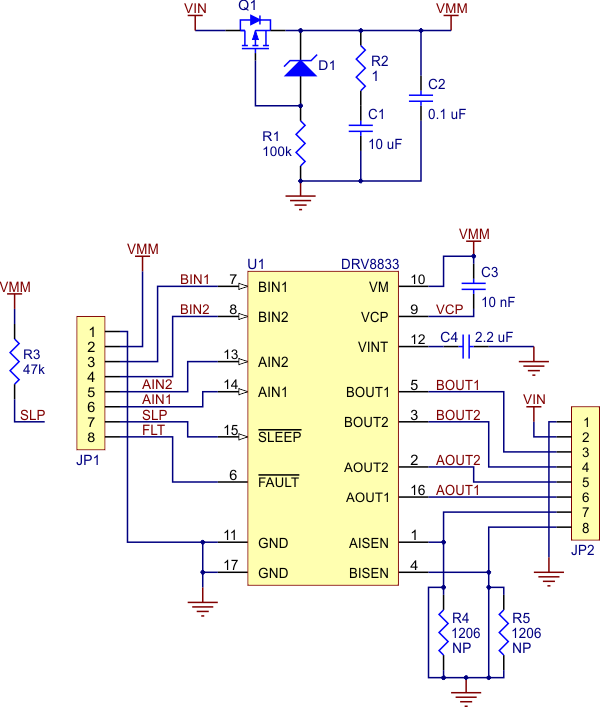
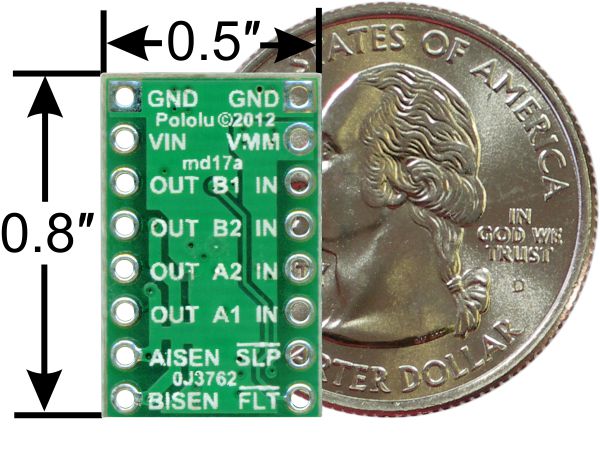
핀아웃
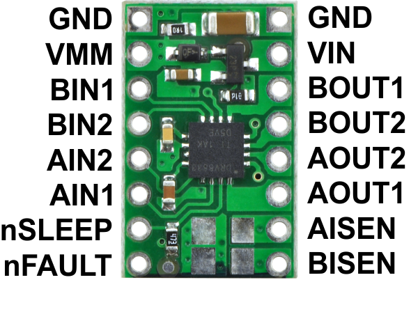
| PIN | Default State | Description |
|---|---|---|
| VIN | 2.7–10.8 V motor power supply connection. Operation with VIN below 5 V slightly reduces the maximum current output. | |
| VMM | This pin gives access to the motor power supply after the reverse-voltage protection MOSFET (see the board schematic below). It can be used to supply reverse-protected power to other components in the system. It is generally intended as an output, but it can also be used to supply board power. | |
| GND | Ground connection points for the motor power supply and control ground reference. The control source and the motor driver must share a common ground. | |
| AOUT1 | The motor A half-bridge 1 output. | |
| AOUT2 | The motor A half-bridge 2 output. | |
| BOUT1 | The motor B half-bridge 1 output. | |
| BOUT2 | The motor B half-bridge 2 output. | |
| AIN1 | LOW | A logic input control for motor channel A. PWM can be applied to this pin. |
| AIN2 | LOW | A logic input control for motor channel A. PWM can be applied to this pin. |
| BIN1 | LOW | A logic input control for motor channel B. PWM can be applied to this pin. |
| BIN2 | LOW | A logic input control for motor channel B. PWM can be applied to this pin. |
| nSLEEP | HIGH | Sleep input: when this pin is driven low, the chip enters a low-power sleep mode. (Labeled SLP on the board silkscreen.) |
| nFAULT | FLOAT | Fault output: driven low in the event of an over-current, over-temperature, or under-voltage condition; floating otherwise. (Labeled FLT on the board silkscreen.) |
| AISEN | Current sense pin for motor A. This pin is connected to ground and does not function by default, but current limiting can be enabled by making the modifications described below. | |
| BISEN | Current sense pin for motor B. This pin is connected to ground and does not function by default, but current limiting can be enabled by making the modifications described below. |
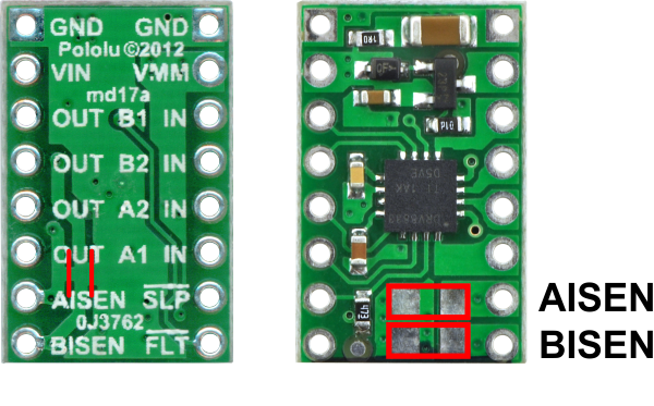
전류 제한
- DRV8833은 고정주파수 PWM current regulation(current chopping)으로 전류를 제한 할 수 있습니다.
- 디폴트로 본 보드는 current sense핀을 그라운드에 연결하여 전류 제한 기능을 비활성화 합니다.
- 전류 제한 기능을 활성화 하려면 아래의 그림과 같이 보드 뒷면의 브레이크 포인트를 칼로 끊고 앞면의 전류 센싱 저항을 납땜하여 주어야 합니다.
- 저항 값이 어떻게 chopping current를 결정하는지는 DRV8833의 데이터쉬를 참고하십시오.
실제 사용시 고려사항
- DRV8833 데이터쉬트는 모터당 연속해서 1.5A의 최대 전류를 공급할 수 있다고 언급하고 있지만, 칩은 더 낮은 전류에서도 뜨거워 집니다.
- 예를 들어, 상온에서 테스트하였을 경우, 칩이 채널당 1.5A를 전류를 공급할 경우 칩이 과열 보호 기능이 시작되기 전까지 1분정도 공급이 가능하며, 1.2-1.3A를 공급할 경우 수분 동안 공급이 가능합니다.
- 그러므로 실제 공급 가능한 전류는 얼마나 칩을 잘 식히느냐에 달려 있습니다.
- 본 제품은 열을 잘 발산하도록 디자인 되어 있지만 heat sink를 추가하면 좀 더 나은 성능을 얻을 수 있습니다.
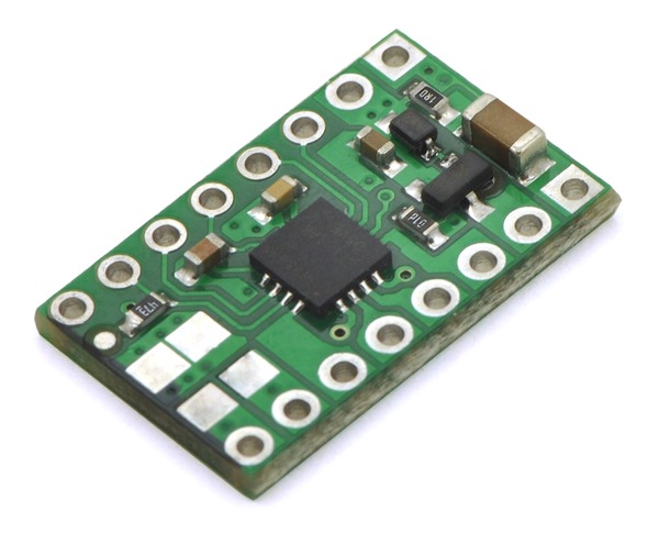
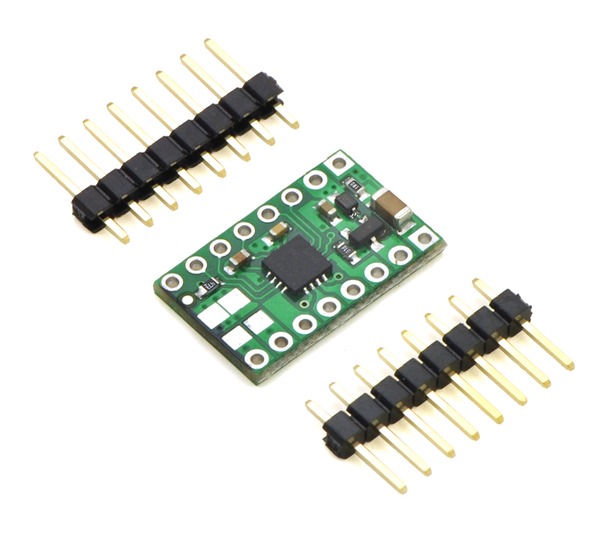
포함된 하드웨어
회로도